Low Voltage Differential Signaling (LVDS) overview
- Posted by Manuel Padial Pérez
- On June 24, 2019
- 1
Low Voltage Differential Signaling (LVDS) technology, include benefits over other technologies, as different kind of devices and configurations available.
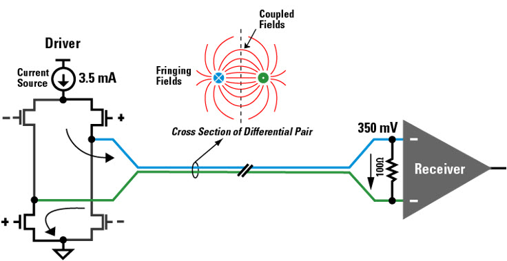
A method to communicate data at high frequency (400Mbits to 4Gbits) using a very low voltage swing (e.g., 350mV) over differential Printed Circuit Board (PCB) traces or a balanced cable.
I/O signal levels are defined by ANSI/TIA/EIA-644
- Standard specifies LVDS as a way to transmit and receive hundreds of megabits per second per channel over differential media
- Protocol independent. i.e., it is an electrical standard only, not defining a protocol. The system architect is responsible for protocol definition.
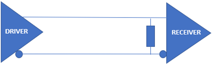
Uses differential signals with low voltage swings to transmit data at high rates over wider lengths
- Differential signals contrast to traditional single-ended signals in that two complementary lines are used to transmit a signal instead of one line.
- Two signals are generated of opposite polarity, and then the data transmission references the two signals to one another.
- This transmission scheme provides the kind of large common-mode rejection and noise immunity to a data transmission system that a single-ended system referenced only to the ground cannot provide.
Requires a terminating resistor (commonly, 100 ohms are employed)
- To prevent reflections
- Matched to the actual cable or PCB trace’s differential impedance
- This resistor, placed across the differential signal lines as close as possible to the receiver input, completes the current loop and properly terminates the signal.
Electrical Characteristics
- 247 mV to 454 mV (nominal 350mV) output
- 100 Ohms load
- 05 V to 2.35 common mode input range
- +/- 100 mV threshold
- 2 mW (3.5 mA x 350 mV)
GET IN TOUCH TODAY!
Do you have questions? Contact us!
Benefits of differential signaling
The differential data transmission method used in LVDS is less susceptible to common-mode noise than single-ended schemes. The differential transmission uses two wires with opposite current/voltage swings instead of the one wire used in single-ended methods to convey data information. The advantage of the differential approach is that if noise is coupled onto the two wires as common-mode (the noise appears on both lines equally) and is thus rejected by the receivers, which looks at only the difference between the two signals.
The differential signals also tend to radiate less noise than single-ended signals due to the canceling of magnetic fields. In addition, the current mode driver is not prone to ringing and switching spikes, further reducing noise. Because differential technologies such as LVDS reduce concerns about noise, they can use lower signal voltage swings. This advantage is crucial because it is impossible to raise data rates and lower power consumption without using low voltage swings. The low swing nature of the driver means data can be switched very quickly. Since the driver is also current-mode, very low – almost flat – power consumption across frequency is obtained. Switching spikes in the driver are very small so that ICC does not increase exponentially as switching frequency is increased.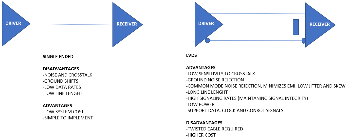
Common-mode noise rejection
- When the two lines of a differential pair run adjacent and in close proximity to one another, environmental noise, such as electromagnetic interference (EMI), is induced upon each line in approximately equal amounts.
- Because the signal is read as the difference between two voltages, any noise common to both lines of the differential pair is subtracted out at the receiver.
- The ability to reject common-mode noise in this manner makes LVDS less sensitive to environmental noise and reduces the risk of noise related problems, such as crosstalk from neighboring lines.
- LVDS can use a much lower voltage swing compared with traditional single-ended schemes that rely on higher voltage swings to maintain an adequate threshold for noise tolerance.
Low Noise
- When the two adjacent lines of a differential pair transmit data, current flows in equal and opposite directions, creating equal and opposite electromagnetic fields that cancel one another. The strength of these fields is proportional to the flow of current through the lines. Thus the lower current flow in an LVDS transmission line produces a weaker electromagnetic field than other technologies.
- Smooth current mode outputs and low demand on power/ground
- Differential fields tend to a couple, reducing EMI
- Noise picked up on differential lines is rejected by the receiver as common mode
High speed over wider lines length
- The reason of this data rate achieving is because of its low output voltage swing, which results in a fast switching slope (RS-422 has a voltage swing of two volts, which results in a slope of around 2ns, but LVDS only has 350 mV resulting in a slope of around 0.8 ns)
- 6μm CMOS provides a path to > than 155Mbps (5.0 devices)
- 25μm CMOS provides a path to > than 400Mbps (3.3 devices)
- 130nm CMOS provides a path to >1250Mbps (2.5V and 1.2 devices)
Low power consumption
- The current-mode driver of LVDS provides a constant 3.5 mA of current through the differential pair. The power consumption at the load can be calculated using the power equation, P = I2R, which states that power is equal to electrical current squared times resistance. Given the 3.5 mA of current through the 100 Ω termination resistor, the power equation results in (3.5 mA)2 x 100 Ohms = 1.225 mW. In comparison, another differential data transmission technology, RS422, dissipates 90 mW of power at the load. Other differential signaling technologies, such as RS485, ECL, and PECL, also dissipate significantly more power than LVDS
- Virtually flat versus frequency
LVDS configurations or topologies
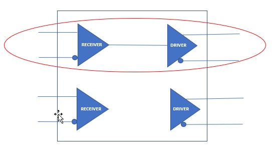
Point to point
Point to point configuration involves only a single driver and receiver pair
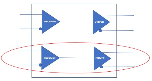
Multiple points to point
Multiple points to point topologies have multiple signal drivers and receivers all sharing a single interconnect
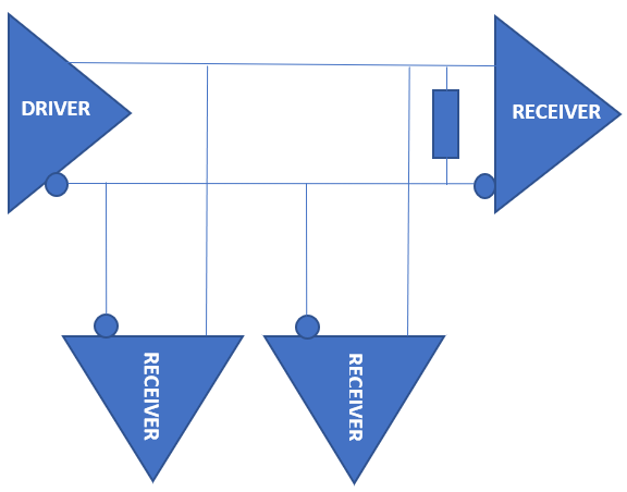
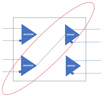
Multi-drop
A variant of multiple point to point topology can include a single driver and multiple receivers
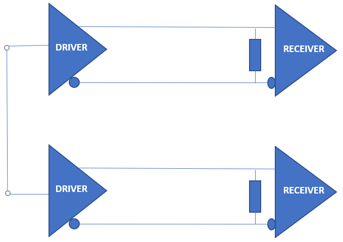
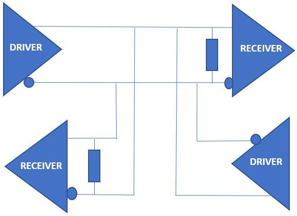
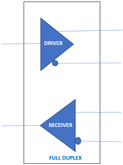
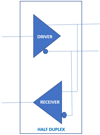
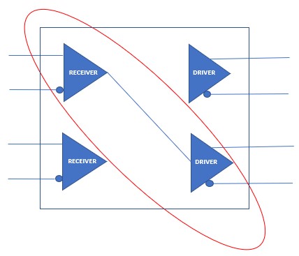
Bi-directional Half duplex
Another variant of multiple points to point topology consists of two driver/receiver pairs that transmit and receive signals between two points over a single interconnect.
LVDS applications
Manufacturers of high-performance analog-to-digital converters (ADCs) and digital-to-analog converters (DACs), use LVDS outputs to transmit digital data at high rates to keep up with the increasing demand for faster sampling rates. One key characteristic of an ADC is that it can accurately convert an analog signal to a corresponding digital representation. Noise radiating from a digital output of the converter can reduce the overall accuracy of the converter by introducing errors at the analog front end. At high sample rates, single-ended outputs generate this kind of harmful noise. LVDS outputs are capable of keeping up with the high data rates and keeping noise emission low, thus protecting the performance of the analog front end. Additionally, some manufacturers have reduced the number of wires necessary to transmit the signals from one point to another by serializing the output bits onto an LVDS pair, which further improves accuracy by avoiding skew-related errors that can occur when transmitting data in parallel.
The low noise emission and high noise rejection characteristics of LVDS make it a practical, reliable choice for military and aerospace applications as well. These applications are often located in harsh, noisy environments with extreme temperatures. LVDS interfaces for avionic communications, surveillance, and intelligence can protect the integrity of the transmitted signals in these environments. In addition, widespread adoption of the standard has produced an abundant supply of LVDS components and devices that make it possible to acquire high-quality, low-cost LVDS parts.
LVDS in space applications
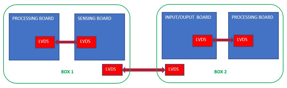
LVDS technology id being widely accepted in space applications solving the increasing demand to move data quickly from box to box or from PCB to PCB within a satellite. Moving large amounts of data requires an extremely high-performance solution that consumes low power, generates little noise and are relatively immune to noise.
Cold sparing
In applications requiring high reliability, cold sparing enables a redundant device to be on the data bus without drawing additional power. The device can be kept in cold spare mode and powered up only when necessary, allowing the application to save power.
These devices are ideal in applications where redundant subsystems are to remain in a high impedance power-off state, which also allows it to be connected to the LVDS bus while being electrically isolated from the data bus.
- When VDD is within 300mV of VSS (0.0 V), the cold spared I/O remain in a high impedance state (> 1MΩ), the cold spare device presents a high impedance to the active signal to avoid signal distortion, so that, the redundant device hangs off an active bus.
- This high impedance does not add significant loading to the active bus, thus interfering very little with the signal.
- Allows for redundant/spare devices to be on the bus
LVDS ecosystem
LVDS driver or transmitter
Consists of a current source output which drives a closely-coupled/spaced differential pair of conductors. Termination resistor at the receiver which matches the differential impedance of the transmission line completes the current loop. The direction of current flow determines the logic level at the receiver.
LVDS receiver
Is a specialized voltage comparator that recognizes the logic state by the voltage polarity across the termination resistor. It is fail-safe, i.e., if the driver loses power, is disabled or is removed from the line, receiver outputs remain in a known state (high).
LVDS transceiver (driver/receiver)
The combination of both, driver and receiver is called transceiver
LVDS Serializer/Deserializer (SerDes)
Serializer/deserializer pairs are used to multiplex a number of low-speed CMOS lines and to transmit them as a single channel running at a higher data rate. SerDes ICs are typically used to reduce the number of connector pins or lines within cables and backplanes. SerDes functions are being embedded into large and complex ICs in order to reduce the number of I/O on the IC package.
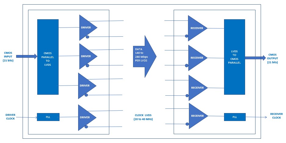
Let´s see an example of converting 21 bits of CMOS data into three LVDS data streams:
- The serializer is a parallel-to-serial converter and converts 7 bits of parallel data to a single LVDS serial data link.
- The deserializer is a serial-to-parallel converter and receives the LVDS data transmitted from the serializer and converts it back into the original 7 bits or parallel data.
- A phase-locked transmit clock is transmitted in parallel with the data streams over a fourth LVDS link
- Every cycle of the transmit clock, 21 bits of input data are sampled and transmitted
- The receiver converts the LVDS data streams back into 21 bits of CMOS data
One of the main advantages of serializing data is skew prevention. Skew is an inherent problem with sending parallel data and its clock across cables or Printed Circuit Boards (PCB) traces. Data and clock recovery are used by the deserializer to extract the serialized data and clock and turn it back into parallel data. Transmitting serial data as opposed to parallel data also reduces the number of interconnect cables or traces required. Thus, reducing the space needed for interconnect.
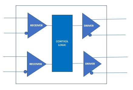
LVDS Crosspoint Switch
Switching architectures are favored over bus architectures when data-rates are high. As a consequence, switches tend to operate at high data rates. LVDS is a common choice for the I/Os on these IC’s. Switches can be used for clock distribution. LVDS is one of the most suitable signaling standards for clocks of any frequency because of reliable signal integrity.
An example of a quad 2×2 Crosspoint Switch has 4 cross-coupled switches:
- Each switch has separate enable and select lines
- Each switch can be configured to be a 1:2 splitter, repeater, crosspoint switch
- It has fully differential data paths from input to output for low noise generation and low pulse with distortion. The non-blocking design allows connection of any input to any output or outputs on each switch.
- This device can be used as a high-speed differential crosspoint, 2:1 mux, 1:2 demux, repeater or 1:2 signal splitter.
- The mux and demux functions are useful for switching between primary and backup circuits in fault-tolerant systems.
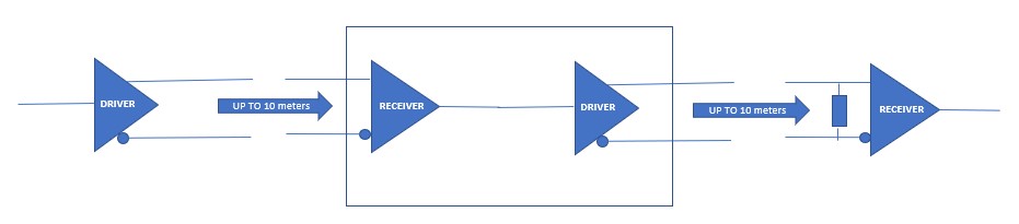
LVDS Repeater or Buffer
Basically, it works as a repeater designed specifically for bridging multiple backplanes in a system, accepting or driving signals onto the local bus.
GET IN TOUCH TODAY!
Do you have questions? Contact us!
Since 2000 in Alter Technology, as EEE Parts Engineer, first in the Engineering and Materials Management Department, has given technical support to customers in many different space programmes. And later on, as Coordinator of the Parts Engineering and Purchasing Department, has been in charge of guarantee the proper EEE Parts selection/definition/testing to ensure the technical/schedule/budget compliance to projects requirements. Currently and since 2017 is leading the Technical Content Maintenance Team of doEEEt platform.
With the continuous maintenance of the platform technical content, doEEEt provides to the space community the most updated and complete information about Hi-Rel EEE components, related documentation, and reports, as well as any associated procurement and testing activities.
- Hi-Rel Intermediate bus converter and point of load - December 11, 2021
- ASIC or FPGA, how to choose between them - October 25, 2021
- Ceramic Hermetic DDR2 SDRAM Memory avalaible for Space - September 13, 2021
1 comments on Low Voltage Differential Signaling (LVDS) overview