Raman Thermometry Technique on Hi-Rel EEE Parts
- Posted by Francisco Javier Aparicio Rebollo
- On March 19, 2020
- 0
As typical length in integrated circuits decreases thermal management is becoming a key factor determining the reliability and lifetime of such systems. Furthermore, micrometric and submicrometric objects in integrated circuits modify local heat transport and may lead to the formation of unintentional hot-spots. Thus, the accurate measurement of the local temperature with micrometric spatial resolution is crucial to confirm the suitable operation of highly integrated systems.

Why Raman Thermometry
The leads of leaded components shall be bent and often cut to the right length before they are mounted/soldered to the substrate. Lead cutting, bending, and mounting are operations that may be hazardous if they are not performed properly.
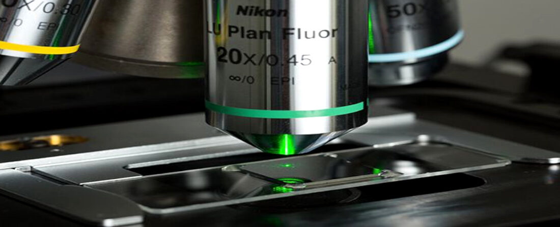
Raman thermometry is a thermal characterization technique that makes use of Raman scattering phenomena to determine the local temperature in microelectronics systems.
Non-contact character.
- High spatial resolution (sub-micron scale).
- In-depth analysis of IR-transparent samples.
- Fast acquisition time, 10 ms to 1 s of exposure to acquiring a full Raman spectrum.
- Temporal resolution as short as hundreds of nanoseconds in dedicated systems
Thanks to these advantages, Raman thermometry is commonly used to study semiconductor devices, polymers, batteries, life sciences, and more.
GET IN TOUCH TODAY!
Do you have questions? Contact us!
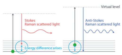
Diagram of Raman Scattering Processes
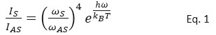
In their spectroscopic facet, Raman techniques are extensively used for the identification of chemical compounds as well as the characterization of the bond structure and solid-state structure of the investigated materials. On the other hand, Raman microscopy has proven to be a useful tool for determining the local temperature in heterogeneous systems. In the most common approach for this application, both the Stokes and Anti-Stokes peaks are registered. Their relative intensities (IS and IAS) are correlated to the local temperature of the illumination spot according to the following equation in the case of solid-state semiconductors, where the and are the frequencies of the Stokes and Anti-Stokes modes and is the frequency of the generated/annihilated phonon.
Practical Applications
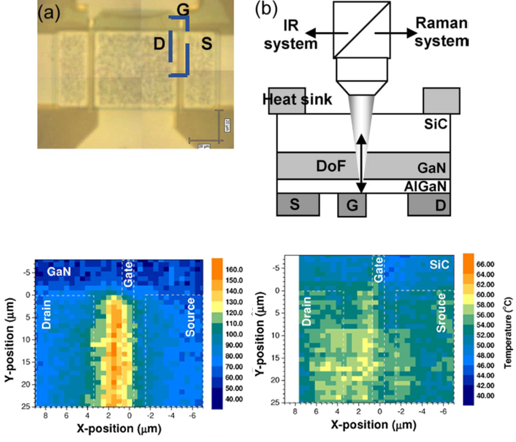
Raman thermal imaging of integrated circuits or other microelectronic devices provides useful information about temperature gradients. The images below show the thermal maps acquired by Raman thermometry in the case of AlGaN/GaN HFET when applying 40V (VSD) and ISD = 25 mA. The Raman thermal maps are registered at different depths; in the GaN layer (boom left) and in the SiC layer (bottom right). The figure illustrates the formation of a hot spot under the region between the gain and the drain that affects in a lesser extent to the temperature distribution within the SiC underlayer.
IEEE TRANSACTION ON ELECTRON DEVICES 0018-9383
Raman temperature map of GaN and SiC layers in an operative HFET systems
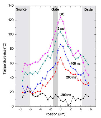
Although the technique is generally applied to steady-state temperature mapping, it is also eventually used to characterize the transient-state temperatures during pulse operation. Time-resolved Raman thermography can be used to measure temperature transients with nanosecond temporal resolution.
The figure shows the transient thermal response of a GaN-on-SiC HEMT measured using time-resolved Raman thermography. It is shown that there is a high-temperature peak between the gate an the drain which leads to the formation of steady state hot spot.
How it works
Raman thermometry is based in the inelastic scattering that a minority of IR phonons experience when they impinge onto a material with the suitable energy to interact with the lattice (phonons) quantized vibration levels. As it is illustrated in the figure during this an unstable “virtual state” is generated and a photon is immediately elastically or inelastically (Raman) scattered. In turns, within Raman scattering we can distinguish between two phenomena, i) Stokes Raman scattering when the emitted photon has lower energy than the incident beam and (phonon generation) ii) Anti-Stokes Raman scattering in which the generated photon absorbs energy from the system (phonon annihilation).
IEEE TRANSACTION ON ELECTRON DEVICES 1530-4388
Time-resolved Raman thermography on 125 micron HEMT located area
Since 2007 Dr. Aparicio has developed a productive research career within the field of Materials Science including post-doctoral stays at the University of Trento, the University of Mons, and the Spanish National Research Council (CSIC). His researches have been published in more than 30 articles in reputed international research journals and conferences (> 70) including more than 10 invited talks and lectures.
Within the frame of the program “Torres Quevedo” for the Knowledge Transfer and the incorporation of research talent into the industry, in 2019 he joined Alter Technology as Senior Materials Science Test Engineer. In 2019 he was appointed to lead the Scanning Acoustic Microscopy Service. Within this framework, he currently collaborates in different ESA projects (JUICE and PLATO).”
Actually, he is not in our company anymore, but still as an external collaborator in our blog.
- Material Analysis Techniques for Electronic Components - May 6, 2022
- SAM: Survey to manufacturers and users - February 17, 2022
- What is a C-SAM Inspection? - January 29, 2022
0 comments on Raman Thermometry Technique on Hi-Rel EEE Parts