RC Snubber Design for SMPS Protection
- Posted by doEEEt Media Group
- On February 13, 2021
- 0
Part II: Design Process and Verification
This part II of the RC Snubber topic discusses the systematic and efficient design process and design verification through simulations and laboratory measurements (see [1] for Part I – fundamentals of inductive switching and RC snubber impact).
Design Process
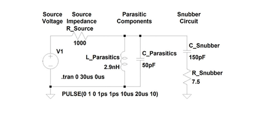
Figure 1 shows the LC resonant circuit with an RC snubber discussed in Part I [1].
Featured Figure 1: LC parasitic circuit with the RC snubber
In this part, we discuss a systematic and efficient design process leading to the choice of the snubber’s capacitor and resistor values shown in Figure 1.

The resonant frequency formula for a circuit without the snubber is [1]
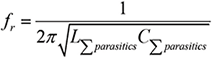
The purpose of using the RC snubber is to suppress the ringing and move the ringing frequency to a lower value (often 50% or less of the original value). Note that in order to half the ringing frequency in Eq. (1), the term under the square root needs to quadruple. If we keep the inductance parasitics constant, the quadruple of the capacitive component can be accomplished by
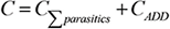
where
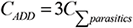
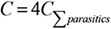
Now the total circuit capacitance, C, is four times the original parasitic capacitance value.
The traditional RC snubber design process consists of the following steps:
Measure the ringing frequency at the switching node, fr
Add a capacitor, CADD, from the switching node to the reference node
Measure the resulting (lower) ringing frequency, fr ‘
Keep changing the added capacitor’s value until the ringing frequency fr ‘ is approximately half of the original ringing frequency, fr, without the added capacitor
This last CADD is the minimum value for the snubber capacitance, Csnub.
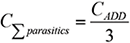
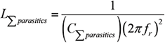
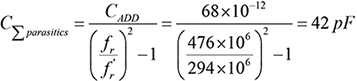
Calculate C∑parasitics
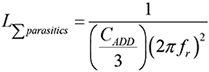
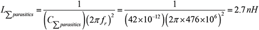
Calculate L∑parasitics
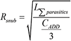
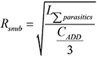
Finally, calculate Rsnub, [2],
Note that this traditional design process requires the substitution of capacitor snubber values to discover CADD by halving fr. This can be easily done in simulations, but not in the actual measurements. The constant changing of capacitor values, hunting for the particular value, is time-consuming and can be destructive.
A faster and more practical method is to try a single capacitor value to determine the circuit’s parasitic capacitance. This process consists of the following steps:
Measure the ringing frequency at the switching node,
Add a capacitor, CADD, from the switching node to the reference node. Pick a value between 47pF and 100pF as a starting point.
Measure the resulting (lower) ringing frequency, fr ‘

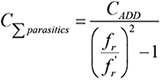
Calculate C∑parasitics
Calculate L∑parasitics
Calculate Csnub,min, [3],
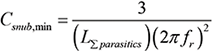
Finally, calculate Rsnub
Design Verification through Simulations
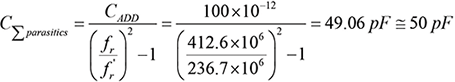
The unsnubbed circuit is shown in Figure 2(a) with the resonant frequency, fr = 412.6 MHz, shown in Figure 2(b), (Step 1).
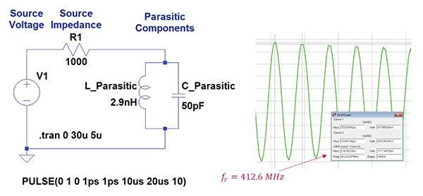
Figure 2(a) shows the circuit with the added capacitance CADD = 100pF with the resonant frequency, fr = 412.6 MHz, shown in Figure 2(b), (Step 2 and 3).
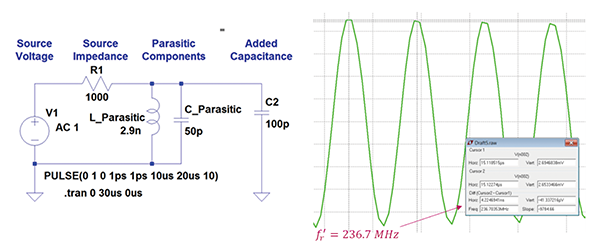
Figure 3: (a) Circuit with added capacitance, (b) resonant frequency
Step 4. Calculate C∑parasitics
Step 5. Calculate L∑parasitics

Step 6. Calculate Csnub,min

Step 7. Calculate Rsnub
These resulting C and R values were implemented in the RC snubber shown in Figure 1. The simulated ringing waveforms for this circuit were discussed in Part I [1], and are repeated here in Figure 4.
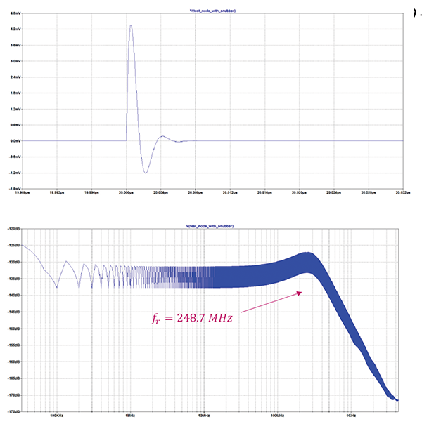
Figure 4: Ringing waveforms with a snubber added: (a) close-up of a time domain waveform, (b) FFT of the waveform
Note that the new ringing frequency of 248.7 MHz is much lower than the original ringing frequency of 412.6 MHz, of the unsnubbed circuit.
Design Verification through Measurements
In this section, we follow the design process of the previous section with the values obtained from measurements (instead of the simulated values).
Figure 5 shows a (redacted) circuit schematic of a buck SMPS with the designed snubber.
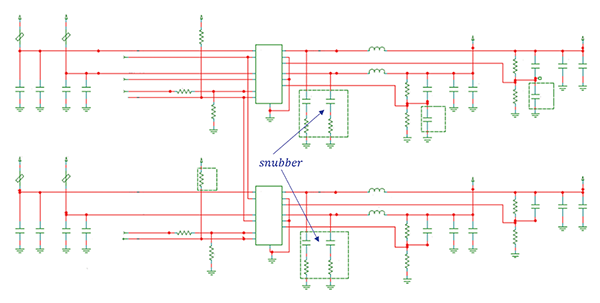
Figure 5: Buck SMPS with a snubber
Figure 6 shows the actual PCB and a differential probe used for measurements [4].
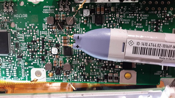
Figure 6: Actual PCB and a differential probe
Figure 7 shows the ringing waveform corresponding to the un-snubbed circuit. The measured ringing frequency is fr = 476.1 MHz (Step 1).
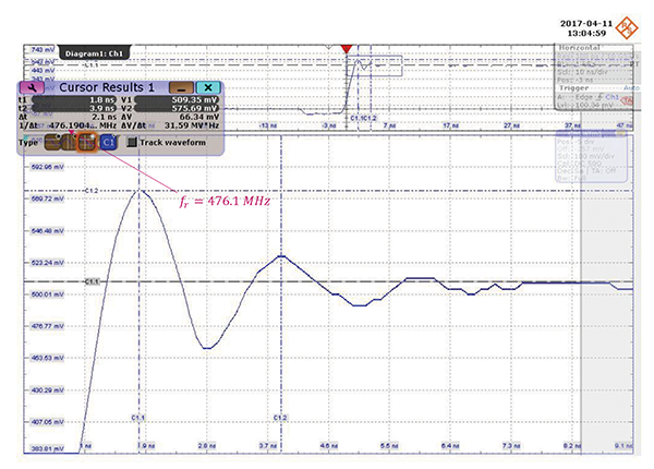
Figure 7: Unsnubbed SMPS: voltage at the switching node
Next, a 68 pF capacitor is added (Step 2). The resulting ringing waveform is shown in Figure 8.
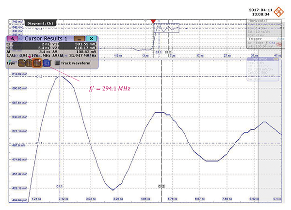
Figure 8: Voltage at the switching node with a C= 68 pF capacitor added
The new (lower) ringing frequency is fr‘ = 294.1 MHz (Step 3).
Step 4. Calculate C∑parasitics
Step 5. Calculate L∑parasitics
Step 6. Calculate Csnub,min

Step 7. Calculate Rsnub
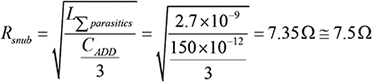
Figure 9 shows the voltage waveform with the C = 150 pF snubber added.
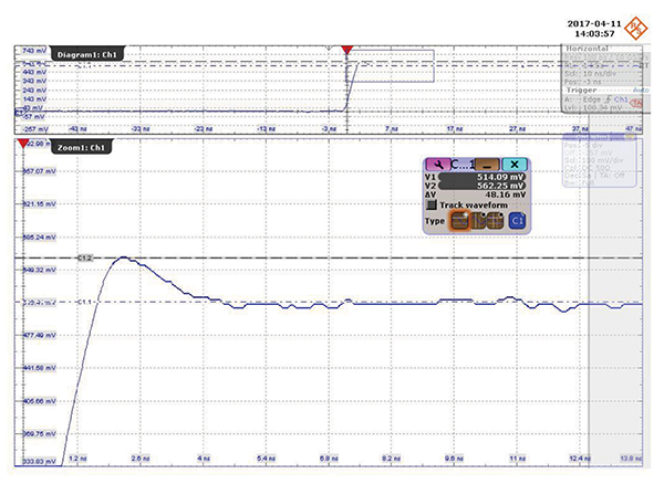
Figure 9: Voltage at the switching node with a C = 150 pF snubber added
Note the decrease in the ringing frequency. Finally, a full RC snubber is implemented (Csnub = 150 pF, Rsnub = 7.5 Ω). The resulting waveform is shown in Figure 10.
Figure 10: Voltage at the switching node with a full RC snubber added
It is evident that the full RC snubber suppressed the ringing at the switching node.
Final Conclusions
It is worth repeating that parasitic inductance in the circuit is distributed over the entire PCB and includes the package inductances. While the snubber components are calculated assuming their effective values, there is no way to physically put them in the circuit to provide ideal damping. The best way to reduce overshoots and ringing is to actually minimize the undesirable inductances in the circuit with good layout practices. Choosing the right low side FETs with low inductance packages and/or integrated Schottky body diodes will offer additional benefits.
Finally, these equations will get you into the ballpark. Differences in leading edge and trailing edge ringing will result in Snubber Circuit component compromises.
Source: In Compliance Mag article
by Bogdan Adamczyk and Bill Spence
A team of experts that brings you the latest and most important news about the EEE Part and Space market.
- New ECSS-Q-ST-60C Standards Explained- Discover - June 4, 2025
- Accelerating Space Missions: Launch Faster with the ZSOM-F01 Rad-Tolerant SoM - June 3, 2025
- Miniature RF Connectors - April 29, 2025
0 comments on RC Snubber Design for SMPS Protection