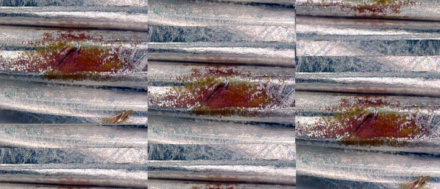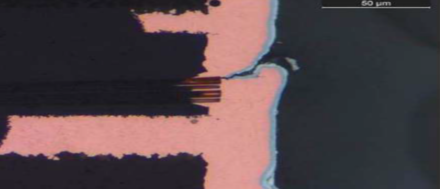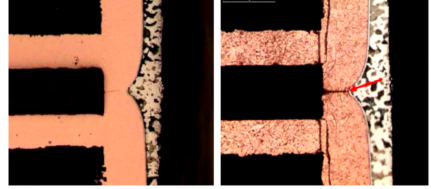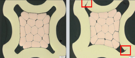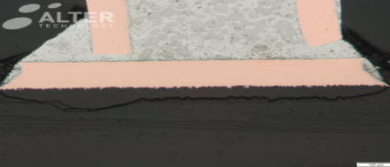
One of the major failure modes encountered in PCB assembly is Pad cratering. This term is coined to describe a fracture at the pad/resin int...
ALTER TECHNOLOGY takes a step further, offering to his customer not only a full set of activities to perform on EEE components, but adding a complementary inspection and validation activities of mounting processes and PCBs.
Materials and Processes laboratory combines accurate characterization techniques and inspection tools with a deep scientific and technological background in materials science. The mission of this area is to thoroughly assess the reliability of materials and processes involved in the manufacturing of spacecraft components.
Materials and Processes task involves three types of interrelated activities.
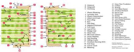
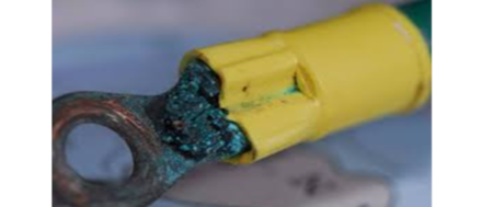
PCB assembly of SMD devices and soldering operations remain amongst the more delicate space-components fabrication task as they may compromise the integrity and performance of the whole system. These processes require specifically trained and skilled operators. Hence ESA pays special attention to the workmanship assessment and has issued specific regulations concerning these issues, ECSS-Q-ST-70-08C and ECSS-Q-ST-70-38C, some of them recently updated.
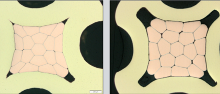
Alter Technology Material and Processes area conduct full soldering and SMD verification test-programs according to the ESCC specifications. For this purpose, our facilities include a fully equipped laboratory to carry out microsectioning inspection together with an environmental laboratory to perform the temperature and vibration test required for PCB and SMD verifications. The facilities and the involved stuff are about to complete the process to become an ESA recommended laboratory to perform these evaluations.
Elemental chemical analyses provide accurate information about the elemental chemical composition of the inspected materials. They are critical in different Hi-REL- verification programs to assess the compliance with the international regulations (e.g. MIL-DTL detail specifications of the USA Defense and Logistic Agency (DLA), ASTM international, NIST standards as well as ESCC regulations of the European Space Agency).
Therefore, they are routinely used to:
On the other hand, fine elemental analysis together with advanced microscopy techniques play a critical role in failure analyses to ascertain and understand the root cause and prevent future fails.
Alter Technology compositional-analyses capabilities cover most of the international regulatory requirements and are adapted to the customer needs in term of:
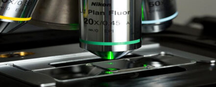
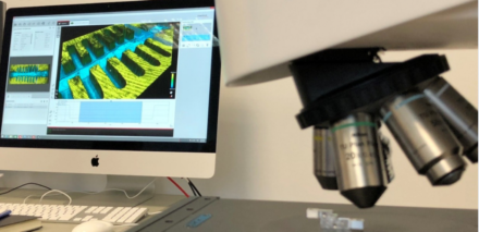
The microscopy facilities available at Alter Technology are perfectly adapted to conduct either conventional inspection task as well as fine analyses requiring advanced instruments. Amongst others, it is worth remaking the FIB capability to perform accurate SEM microsection inspections on semiconductor systems.
Click here and enter in Virtual Lab