Logo
  • Resources
    • COTS for Space WEBINARS
    • ACCEDE 2022 Workshop on COTS
    • EEE COMPONENTS
    • SPECIFICATIONS / QPLs
    • EVENTS / WEBINARS
    • SPACE TALKS
    • TECH ARTICLES
    • MANUFACTURERS NOTIFICATIONS
  • Laboratory Services
    • LABORATORY STANDARD TESTING
    • NON STANDARD TESTING
    • SILICON CARBIDE -SiC- DIODES
    • CROWDTESTING
    • OPTOELECTRONICS
    • SMALL SATS
    • REPRESENTATIVE PROJECTS / PAPERS
  • Additional Services
    • INDUSTRY 4.0 CYBERSECURITY (IEC 62443)
    • PENETRATION TEST
    • CYBERSECURITY CERTIFIED (CSC)
    • CODE SCORE MATRIX
    • LONG-TERM STORAGE OF WAFERS
    • ELECTRONIC DESIGN
  • Tools
    • COMPARATOR
    • MY DCLs/BOMs
    • STOCKPLACE
  • About Us
  • My Request
  • Sign In
Blog Image
Assembly Processes, Packaging and Assembly, Packaging Design, Plastic Packaging for Space

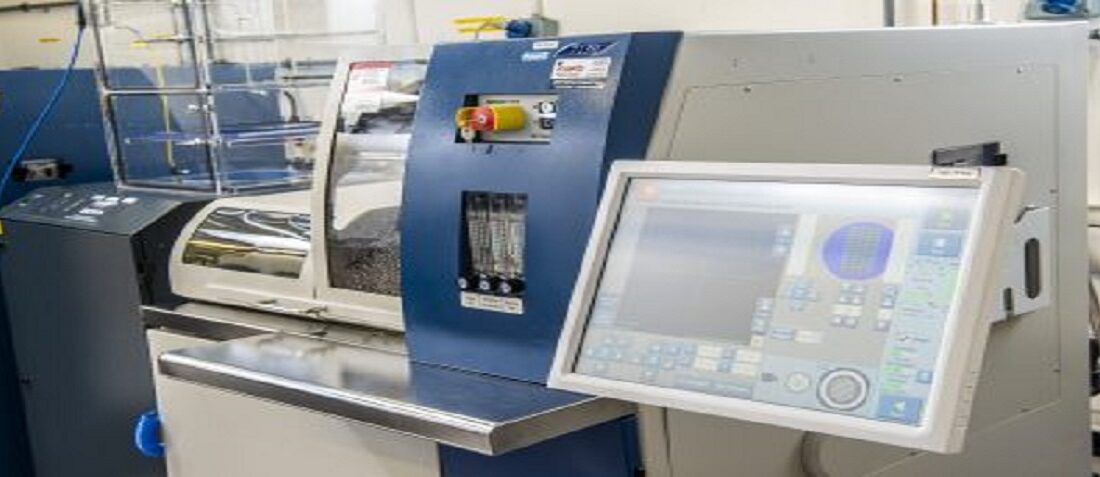
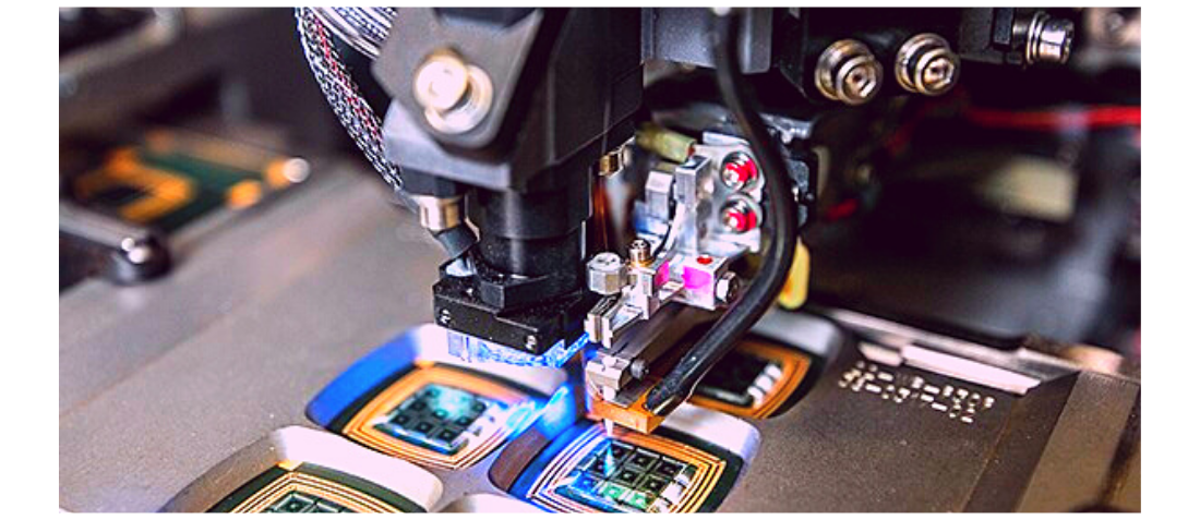
A Bonding Relationship – K&S IConn ProCu PLUS & Alter Technology UK

  • Posted by doEEEt Media Group
  • On July 28, 2021
  • 0
Offering end-to-end backend semiconductor manufacturing, from wafer singulation to assembled product, the company’s design and process IP enables customers to reduce development and manufacturing costs plus reduce time to market.
Read More
Blog Image
Packaging and Assembly, Packaging Applications

Flip Chip

  • Posted by doEEEt Media Group
  • On November 12, 2020
  • 0
Flip chip (also known as direct chip attach) is the process whereby a semiconductor die is attached bond pad side down to a substrate or carrier. The electrical connection is made by means of a conductive bump on the die bond pad.
Read More
Blog Image
Packaging and Assembly, Packaging Design

Package Design and Modelling

  • Posted by doEEEt Media Group
  • On March 16, 2020
  • 0
Alter Technology UK, mechanical design experience covers custom hermetic packages, precision optical benches, heat spreaders, sub-mounts, high power laser coupling.
Read More
Blog Image
Packaging and Assembly, Packaging Design

Optical design

  • Posted by doEEEt Media Group
  • On March 16, 2020
  • 0
Alter Technology UK, optical design capabilities are rooted within the laser and photonics industries for EEE components
Read More
Blog Image
Assembly Processes, Packaging and Assembly

Encapsulation and Hermetic sealing

  • Posted by doEEEt Media Group
  • On March 16, 2020
  • 0
Encapsulation is the process to protect die from damage after die attach and wire bond. There are two main types of encapsulation: Glob Top and Dam and Fill.
Read More
Blog Image
Assembly Processes, Packaging and Assembly

Stud Bumping

  • Posted by doEEEt Media Group
  • On March 16, 2020
  • 0
Gold stud bumping forms Au bumps using a process very similar to Au ball wire bonding. Like wire bonding it forms an Au ball (stud). However, the wire is terminated after the first bond so there is only a bump on the die.
Read More
Blog Image
Assembly Processes, Packaging and Assembly

Wire Bonding Services

  • Posted by doEEEt Media Group
  • On March 16, 2020
  • 0
Alter Technology UK, works closely with our customers at the package design stage to ensure that design for manufacturing techniques are applied and wire bond design rules, where possible, are adhered to. This co-design activity is crucial in the development of a high-yield, fully automated, and fully optimized wire bond process.
Read More
Blog Image
Assembly Processes, Packaging and Assembly

Die Bonding Services

  • Posted by doEEEt Media Group
  • On March 16, 2020
  • 0
Die bonding is the process of attaching a die to substrate/package. Selection of the optimal die attaches material and process is based on a number of issues including thermal requirements, electrical requirements and mechanical stability.
Read More
Blog Image
Assembly Processes, Packaging and Assembly

Pick and Place

  • Posted by doEEEt Media Group
  • On March 13, 2020
  • 0
Alter Technology UK, has the capability to pick and place die from a variety of presentation formats with placement accuracies ranging from 1um to 15um.
Read More
Blog Image
Assembly Processes, Packaging and Assembly

Wafer Sawing

  • Posted by doEEEt Media Group
  • On March 13, 2020
  • 0
Wafer Sawing is the process of singulating the wafer into individual dies ready for subsequent assembly. Alter Technology UK has the capability for Wafer saw of substrates up to 8” diameter. When dicing of substrates of 12” diameter is required then ATN UK can process 12” substrates into smaller segments prior to dicing.
Read More
Page 1 of 3123
Recent Posts
  • Miniature RF Connectors
  • Miniature RF Connectors for high-performance testing
  • Space-Grade components available for immediate delivery
  • Introduction to RD ALFA Microelectronics: Components and Capabilities
  • Managing EEE components for LEO and lower cost space missions
Scroll

doEEEt.com

DoEEEt: Electrical Electronic Electromechanical (EEE) parts database. Find (EEE) components/parts products and datasheets from hundreds of manufacturers.

Privacy Policy and Legal Notice

Copyright

Cookie Policy

Copyright © 2021 ALTER TECHNOLOGY TÜV NORD S.A.U

Company

About us

Contact us

How does doEEEt works? – FAQ

ALTER Laboratory Services

Microwave and RF Testing

Small Sats Testing

COTS components Testing

Authenticity Test