Logo
  • Resources
    • COTS for Space WEBINARS
    • ACCEDE 2022 Workshop on COTS
    • EEE COMPONENTS
    • SPECIFICATIONS / QPLs
    • EVENTS / WEBINARS
    • SPACE TALKS
    • TECH ARTICLES
    • MANUFACTURERS NOTIFICATIONS
  • Laboratory Services
    • LABORATORY STANDARD TESTING
    • NON STANDARD TESTING
    • SILICON CARBIDE -SiC- DIODES
    • CROWDTESTING
    • OPTOELECTRONICS
    • SMALL SATS
    • REPRESENTATIVE PROJECTS / PAPERS
  • Additional Services
    • INDUSTRY 4.0 CYBERSECURITY (IEC 62443)
    • PENETRATION TEST
    • CYBERSECURITY CERTIFIED (CSC)
    • CODE SCORE MATRIX
    • LONG-TERM STORAGE OF WAFERS
    • ELECTRONIC DESIGN
  • Tools
    • COMPARATOR
    • MY DCLs/BOMs
    • STOCKPLACE
  • About Us
  • My Request
  • Sign In
Blog Image
Packaging and Assembly, Packaging Applications

Flip Chip

  • Posted by doEEEt Media Group
  • On November 12, 2020
  • 0
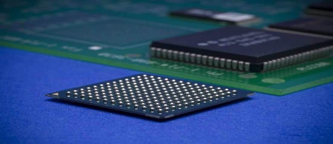
Flip chip (also known as direct chip attach) is the process whereby a semiconductor die is attached bond pad side down to a substrate or carrier. The electrical connection is made by means of a conductive bump on the die bond pad.
Read More
Packaging and Assembly, Packaging Applications

MEMS Packaging

  • Posted by doEEEt Media Group
  • On March 12, 2020
  • 0
Alter Technology UK, has experience in the assembly and packaging of MEMS devices. Our Labs offers customers support in both prototype/process development for LED packaging
Read More
Packaging and Assembly, Packaging Applications

Laser Diode Packaging

  • Posted by doEEEt Media Group
  • On March 12, 2020
  • 0
Alter Technology UK, offers customers support in both prototype/process development for laser diode packaging as well as volume manufacturing capability.
Read More
Packaging and Assembly, Packaging Applications

Image Sensor Assembly

  • Posted by doEEEt Media Group
  • On March 12, 2020
  • 0
Alter Technology (formerly Optocap), Image Sensor assembly platform is a flexible solution for CMOS, CCD and Focal Plane Array sensor chips into ceramic packages.
Read More
Packaging Applications

LED CHIP On Board

  • Posted by doEEEt Media Group
  • On March 12, 2020
  • 0
Why LED Chip-on-Board? Cost-effective alternative to incandescent and fluorescent light sources Increased life span and efficiency System integration, no user-serviceable parts The reduced total cost of ownership Customised array size and shape Application-specific wavelengths
Read More
Packaging and Assembly, Packaging Applications

System In Package

  • Posted by doEEEt Media Group
  • On March 12, 2020
  • 0
The semiconductor industry requires higher levels of integration, lower costs and greater functionality to meet the demands of consumer and industrial products.
Read More
Packaging and Assembly, Packaging Applications

Chip on Board

  • Posted by doEEEt Media Group
  • On March 12, 2020
  • 0
Chip on Board assembly is the process whereby a bare semiconductor die is mounted on a printed circuit board or substrate using conductive or non-conductive epoxies.
Read More
Packaging and Assembly, Packaging Applications

QUANTUM

  • Posted by doEEEt Media Group
  • On March 12, 2020
  • 0
Quantum technology applications such as atomic clocks, magnetometers and gravitometers are now emerging from the laboratory and confronting the challenging size, weight, power, cost and reliability demands of the real-world.
Read More
Packaging and Assembly, Packaging Applications

Photonic Integrated Circuit (PIC) Packaging

  • Posted by doEEEt Media Group
  • On March 11, 2020
  • 0
A PIC is a photonic integrated circuit that integrates multiple photonic functions, such as lasers, detectors, modulators and splitters on a single chip.
Read More
Recent Posts
  • Miniature RF Connectors
  • Miniature RF Connectors for high-performance testing
  • Space-Grade components available for immediate delivery
  • Introduction to RD ALFA Microelectronics: Components and Capabilities
  • Managing EEE components for LEO and lower cost space missions
Scroll

doEEEt.com

DoEEEt: Electrical Electronic Electromechanical (EEE) parts database. Find (EEE) components/parts products and datasheets from hundreds of manufacturers.

Privacy Policy and Legal Notice

Copyright

Cookie Policy

Copyright © 2021 ALTER TECHNOLOGY TÜV NORD S.A.U

Company

About us

Contact us

How does doEEEt works? – FAQ

ALTER Laboratory Services

Microwave and RF Testing

Small Sats Testing

COTS components Testing

Authenticity Test