
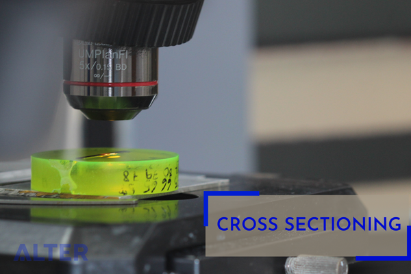
Cross Sectioning for Film Resistors
The cross-sectioning process provides access to the device internal structure, its materials and design. Electronics components are often subjected to cross-sectioning to detect the defects that could not be found using other testing techniques. Cross-sectioning typically involves three discrete steps: mounting the sample in a block of epoxy resin to form the specimen, grinding or cutting the specimen and finally polishing the exposed surface. >> Read more


EEE Parts Results Page
Cross Sectioning for Film Resistors
The cross-sectioning process provides access to the device internal structure, its materials and design. Electronics components are often subjected to cross-sectioning to detect the defects that could not be found using other testing techniques. Cross-sectioning typically involves three discrete steps: mounting the sample in a block of epoxy resin to form the specimen, grinding or cutting the specimen and finally polishing the exposed surface. >> Read more
EEE Parts Results Page
17121749 results found for Film/Resistors
Part reference
Quality level / QPL
Package
Power Rating
Resistance [Nom]
Temperature Coefficient of Resistance
Tolerance
Unit price
Lead time
FAILURE RATE S
Qualified
QPDSIS-55342
Surface Mount
Chip
1505 (3812 Metric)
150mW
105K
±300ppm/ºC
±1%
LEVEL V
Qualified
QPDSIS-55342
Surface Mount
Chip
2512 (6432 Metric)
1W
330R
±100ppm/ºC
±5%
LEVEL U
Qualified
QPDSIS-55342
Surface Mount
Chip
0502 (1406 Metric)
50mW
931R
±25ppm/ºC
±0,1%
LEVEL U
Qualified
QPDSIS-55342
Surface Mount
Chip
2208 (5720 Metric)
225mW
517K
±100ppm/ºC
±0,5%
NON-ER
Qualified
QPDSIS-55342
Surface Mount
Chip
2512 (6432 Metric)
1W
1K30
±300ppm/ºC
±1%
LEVEL V
Qualified
QPDSIS-55342
Surface Mount
Chip
0505 (1412 Metric)
125mW
47K0
±100ppm/ºC
±10%
LEVEL T
Qualified
QPDSIS-55342
Surface Mount
Chip
1005 (2512 Metric)
200mW
160K
50ppm/ºC
±5%
LEVEL T
Qualified
QPDSIS-55342
Surface Mount
Chip
2208 (5720 Metric)
225mW
673R
±200ppm/ºC
±0,5%
FAILURE RATE P
Qualified
QPDSIS-55342
Surface Mount
Chip
0502 (1406 Metric)
50mW
12K4
±100ppm/ºC
±0,25%
NON-ER
Qualified
QPDSIS-55342
Surface Mount
Chip
0705 (1712 Metric)