
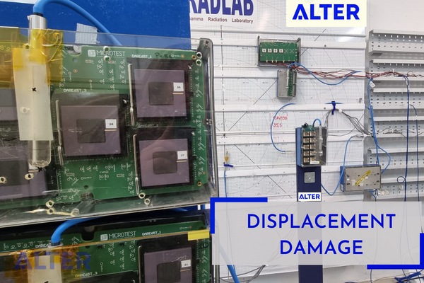
Displacement Damage Test for Analog Switch
Displacement Damage is the result of nuclear interactions, typically scattering, which cause lattice defects. This effect degrades minority carrier lifetime; a typical effect would be gain degradation and leakage current in bipolar transistors. Displacement damage depends on the loss of non-ionizing energy , i.e. energy and momentum transfer to lattice atoms, which depends on the mass and energy of the incident quanta. A simple measure like for ionizing radiation is not possible, so displacement damage must be specified for a specific particle type and energy. >> Read more


EEE Parts Results Page
Displacement Damage Test for Analog Switch
Displacement Damage is the result of nuclear interactions, typically scattering, which cause lattice defects. This effect degrades minority carrier lifetime; a typical effect would be gain degradation and leakage current in bipolar transistors. Displacement damage depends on the loss of non-ionizing energy , i.e. energy and momentum transfer to lattice atoms, which depends on the mass and energy of the incident quanta. A simple measure like for ionizing radiation is not possible, so displacement damage must be specified for a specific particle type and energy. >> Read more
EEE Parts Results Page
343 results found for Analog Switch/Signal Acquisition-Conditioning/Microcircuits
Part reference
Quality level / QPL
Package
Unit price
Lead time
JAN B
Not qualified
QPDSIS-38535
Through Hole Mount
CDIP-14
JAN B
Not qualified
QPDSIS-38535
Through Hole Mount
TO-100
883
Not qualified
NOT LISTED IN QPL
Through Hole Mount
CDIP-14
883
Not qualified
NOT LISTED IN QPL
Through Hole Mount
CDIP-14
883
Not qualified
NOT LISTED IN QPL
Through Hole Mount
CDIP-16
883
Not qualified
NOT LISTED IN QPL
Through Hole Mount
CDIP-16
883
Not qualified
NOT LISTED IN QPL
Surface Mount
CQLCC-20
883
Not qualified
NOT LISTED IN QPL
Through Hole Mount
CDIP-14
883
Not qualified
NOT LISTED IN QPL
Through Hole Mount
TO-100
JAN B
Not qualified
QPDSIS-38535
Through Hole Mount
TO-100
Part validation activities
Cost & Activity Matrix