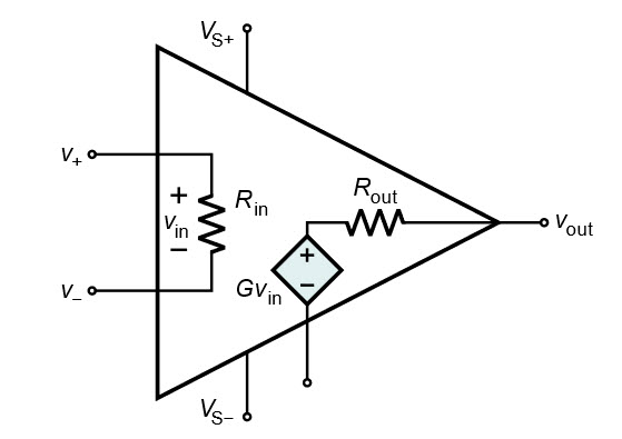
Despite ideally the op-amps have zero current at the inputs, zero input and output offsets, infinite gain, infinite speed, infinite output current and unlimited input/output range, in reality, these parameters are limited.

Fig.1. An equivalent circuit of an operational amplifier that models some resistive non-ideal parameters. (source: wikipedia.org)
Therefore, these parametric characteristics determine the real behaviour of the part type. The evolution of these parameters under several stress conditions must be monitored to ensure proper performance in space applications. The most typically used as performance indicators:
Input Bias Current: This is the minimal current flowing in or out of the input pins. This is important if dealing with low currents in the stage before the op-amp. However, it can also be used as an indicator of the start of performance degradation due to stress, as this type of leakage current is sensitive to stresses such as radiation.
Input Offset Current: This is the difference between the bias current of the two inputs.
Output Offset Voltage: This is the difference between its ideal DC output and its actual DC output when the input is set to some fixed reference value, usually ground or middle-range voltage.
Input Offset Voltage: This is the voltage that must be applied to the input to restore the output to the ideal level, i.e. analogue ground or middle-range voltage.
Slew Rate: This is the maximum rate of change of voltage at its output. This is particularly important when using the op-amp with abrupt signals, such as clocks or image sensors’ outputs.
Bandwidth: This expresses the frequency response in the form of Closed-Loop Large/Small Signal 3dB Bandwidth or Gain Bandwidth Product in a voltage feedback op-amp, where the product of the closed-loop gain and the 3dB closed-loop bandwidth at that gain is a constant.
Open-Loop Gain: This is the gain of the op-amps without positive or negative feedback.
Common Mode Rejection Ratio (CMRR): If a differential input voltage is applied, ideally the output should not be affected by the standard mode voltage, i.e. the average absolute voltage value between both inputs’ values. The CMRR is the ratio between the common-mode gain and the differential mode gain.
Power Supply Rejection Ratio (PSRR): This indicates the ability to have the output unaltered by variations of the power supply. The PSRR is the ratio between the voltage change in the power supply to the voltage change produced in the production.
Input Common-Mode Voltage Range: This is the range of common-mode input voltage that, if exceeded, will cause the total harmonic distortion of the output signal resulting from the common-mode input to exceed a specified maximum or minimum value.
Output Voltage Swing: This the peak positive or negative output, referred to zero, that can be obtained without waveform clipping.
Quiescent Current: This is the power supply current that it is consumed usually with output disable or output current nearly zero. This parameter is a tremendous global indicator of changes in the device.
Input Voltage Noise: This is the internal noise voltage reflected an ideal voltage source in the input pins at a specific frequency. The value is expressed in units of volts per the square root of hertz. Usually is a point of the frequency characteristics curve of noise just after the flicker noise and at the beginning of the white noise. This varies between 1nV/√Hz to 20nV/√Hz.
Input Current Noise: This is similar to the previous one but in the form of currents at the inputs. Current noise varies more widely than voltage noise, as dependent upon the input structure. It can vary between 0.1fA/√Hz to several pA/√Hz.
Sonia Vargas
She works as responsible for the mixed signal test development area, focusing on ASICs and complex systems test design for aerospace applications.
