Optocoupler provided isolation between circuits that need to have interaction in between. To make a good circuit design, we have to know all about the main parameters of an optocoupler and understand the specification.
Circuit Design: Main parameters of an optocoupler
Absolute maximum ratings
These parameters are fundamental for the functionality of the device. They define the admissible limit of operation.
- Operating and Storage Temperature: Ambient temperature in which the device (powered) functions standardly, space applications round -55°C to +125°C. Storage temperature refers to the temperature range that supports the component when it is not powered, -65°C to +150°C in space environments.
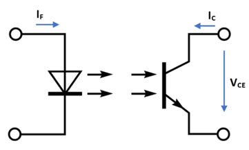
- Power dissipation: The amount of energy that the device can safely dissipate. Power decreases with increasing ambient temperature, generally reaching its maximum at the nominal ambient temperature. Optocoupler dissipates power through the Light-Emitting Diode and the phototransistor in the function of LED’s forward current and forward voltage and phototransistor’s collector current, collector-to-emitter voltage.
- Isolation Voltage: Consists of the maximum voltage that can be applied between an optocoupler’s input and output. It is defined by a specific input signal in a limited time and refers to the capacity of isolation resistance of the device.
- Forward current (IF): maximum current allowed by the LED, within limits power dissipation range.
- Reverse Voltage (VR): maximum reverse voltage allowed by the LED. If the reverse voltage exceeds, a reverse current will flow in the device. This may occasionally degrade or even destroy.
- Collector current (IC): the maximum current that can flow through the phototransistor when it is activated by the LED. As before, the maximum power dissipation must be considered.
- Collector to Emitter Voltage (VCE): Maximum differential potential between collector and emitter of a phototransistor when LED does not emit (IF=0, IB=0).
- Emitter to Collector Voltage (VEC): maximum reverse voltage allowed by the phototransistor.
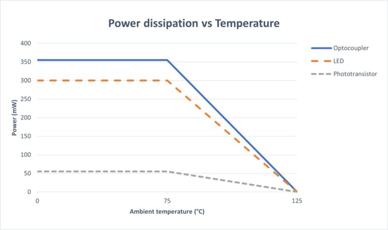
A balance of the parameters discussed above is necessary for long device life. Exceeding the limit of any of the maximum ratings could result in degradation and even non-recoverable degradation of the component.
Electrical characteristics
Otherwise, the principal electrical characteristics of an Optocoupler are:
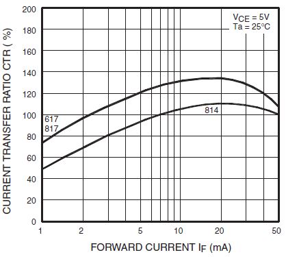
- Current Transfer Ratio (CTR): represents, expressed in percentage, the ratio between the output current (IC) and the input current (IF) of an optocoupler.

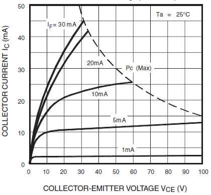
LED Forward current, ambient temperature, or phototransistor collector to emitter voltage influences the CTR, causing variation. In addition, aging also affects this parameter. The specification usually includes graphs of the variation of the CTR based on those as mentioned above, for example:
- Forward Voltage (VF): Differential potential of the LED when a current flows through it (emitter side). Increasing forward current or the falling ambient temperature causes increases in forwarding voltage.
- Reverse Current (IR): the leakage current leakage when a reverse voltage (within the maximum rating) is applied to the LED. Note that this value will increase with increasing reverse voltage and ambient temperature.
- Off-state collector current (IC(OFF)): the leakage current of the collector when LED does not emit (IF=0, IB=0). This value will increase with increasing the power supply and ambient temperature.
- Collector Saturation Voltage (VCE(SAT)): Describe de maximum voltage that will be dropped across the phototransistor when it is in saturation mode.
Time characteristic
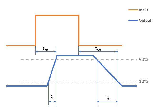
- Rise Time and Fall Time (tr, tf): Time is taken by the optocoupler’s output signal to switch state. The Rise Time represents the time the output signal rises from 10% to 90% and the Fall Time represents the time the output signal falls 90% to 10%.
- Propagation delay time (tp): defines the time it takes for the optocoupler output to respond to a change in the input signal.
