Logo
  • Resources
    • COTS for Space WEBINARS
    • ACCEDE 2022 Workshop on COTS
    • EEE COMPONENTS
    • SPECIFICATIONS / QPLs
    • EVENTS / WEBINARS
    • SPACE TALKS
    • TECH ARTICLES
    • MANUFACTURERS NOTIFICATIONS
  • Electronic Design
  • Laboratory Services
    • LABORATORY STANDARD TESTING
    • NON STANDARD TESTING
    • SILICON CARBIDE -SiC- DIODES
    • CROWDTESTING
    • OPTOELECTRONICS
    • SMALL SATS
    • REPRESENTATIVE PROJECTS / PAPERS
  • Tools
    • COMPARATOR
    • MY DCLs/BOMs
    • STOCKPLACE
  • About Us
  • My Request
  • Sign In
Blog Image
INSPECTION, ELECTRICAL & VERIFICATION, TESTING

Using a Fluorescence Microscopy + dye penetrant test on EEE Parts

  • Posted by Francisco Javier Aparicio Rebollo
  • On February 19, 2021
  • 0
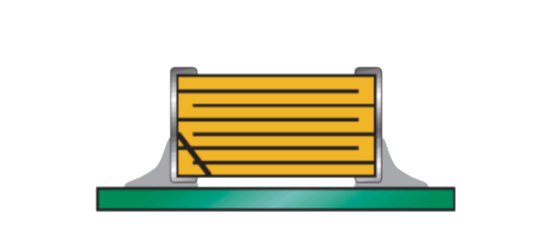
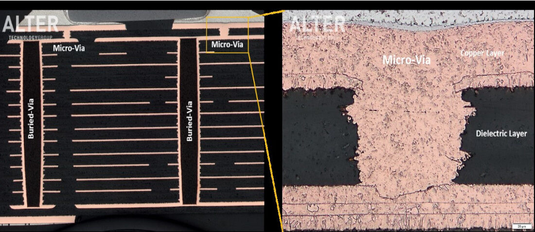
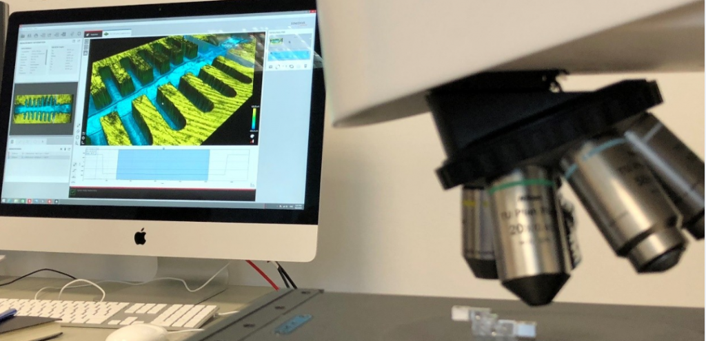
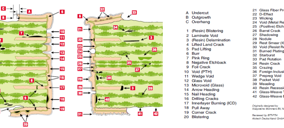
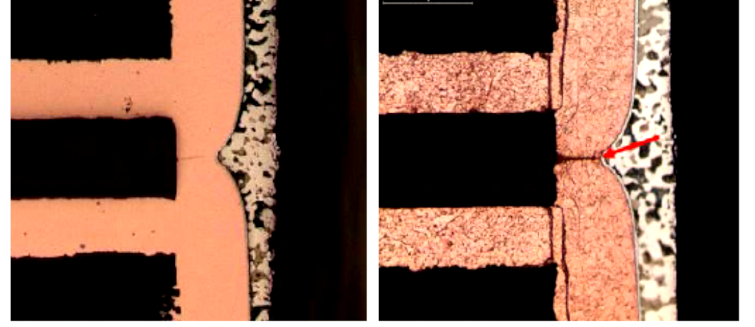
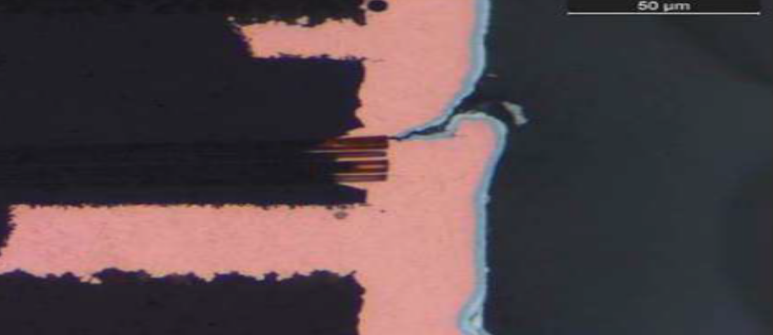
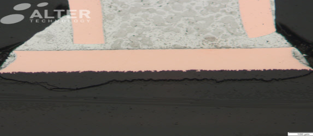
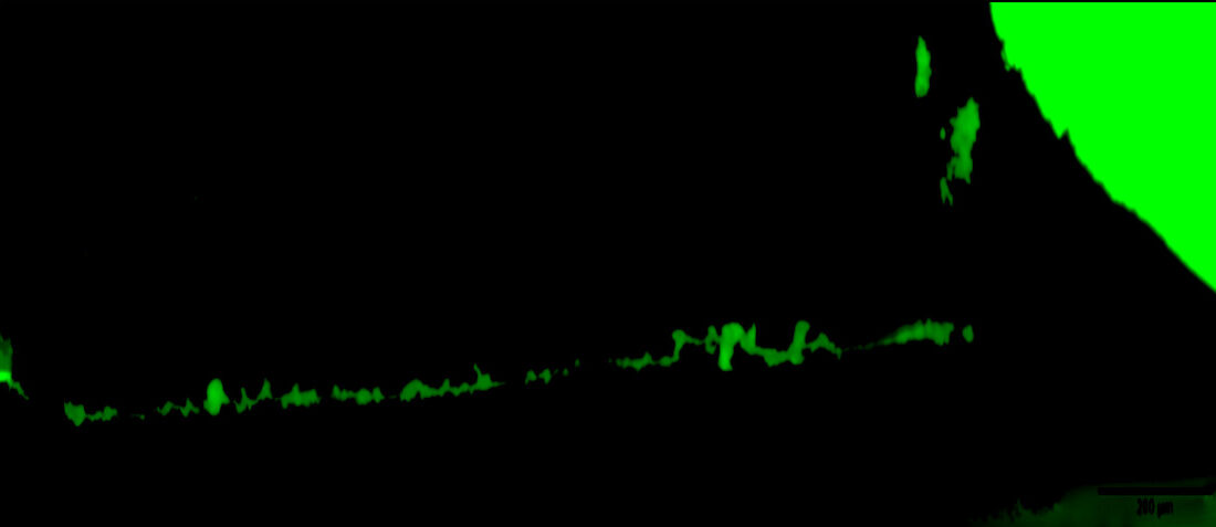
The Fluorescence Microscopy + dye penetrant test is a technique that combines two inspection methods commonly used for the detection of surface anomalies such as cracks, porosity, laps, delaminations, and other discontinuities.
Read More
Blog Image
ABC of CLR, EEE Components, PASSIVES, PHYSICAL, MECHANICAL & ASSEMBLY, TESTING

Mounting Guidelines: Soldering, PCB Handling & Rework

  • Posted by Tomáš Zedníček
  • On October 18, 2020
  • 1
What are the optimum soldering conditions and solder fillet? The best solder fillet for all SMT applications is one which makes a reliable connection and which best withstands the environmental exposures of the products with minimum degradation. This fillet is difficult to describe quantitatively for all parts. The optimum fillet ranges in height from about 1/3 to 2/3 of the part termination height. This does not mean that all solder joints outside of this range should be repaired. It does mean that this is the target for the process engineer to reach for in his process. As many as possible of the solder fillets on the board should be in this range.
Read More
Blog Image
Microsectioning - Short Technical Notes, PHYSICAL, MECHANICAL & ASSEMBLY, TESTING

Evaluation of PCB in Alter Technology Lab.

  • Posted by Mari Carmen López
  • On July 25, 2020
  • 0
The separation of the interest area has to be performed in such a way as to prevent any damage by deformation or input of heat. After cleaning, the specimen is encapsulated before the grinding process takes place.
Read More
Blog Image
INSPECTION, ELECTRICAL & VERIFICATION, TESTING

Need a 3D Characterization Testing? Use Scanning Microscopy CLSM

  • Posted by Fernando Teberio
  • On July 2, 2020
  • 1
Modern manufacturing techniques depend on 3D measurement data combined with CAD/CAM techniques for quality control of high-precision components or mass production. Typically, contact measurement has been widely utilized by the industry. However, for complex and small 3D structures, the application of contact measurement is cumbersome or sometimes impossible. Therefore, noncontact measurement has gradually received much attention from researchers and industry.
Read More
Blog Image
INSPECTION, ELECTRICAL & VERIFICATION, PHYSICAL, MECHANICAL & ASSEMBLY, TESTING

Studying Critical elements in PCB systems: Plated Through Via (PTV)

  • Posted by Mari Carmen López
  • On March 13, 2020
  • 0
Plated Through Vias (PTV) are critical elements in PCB systems and special care must be paid during their inspection in order to ensure the reliability, as they are one the main factors that determine the PCB Quality. The functionality and reliability of PTVs are dictated by: the plated through hole architecture (height/diameter), plating (thickness and quality) and other PCB general characteristics (materials and design).
Read More
Blog Image
INSPECTION, ELECTRICAL & VERIFICATION, PHYSICAL, MECHANICAL & ASSEMBLY, TESTING

Plated Through Via (PTV) Manufacturing Defects

  • Posted by Mari Carmen López
  • On March 13, 2020
  • 0
The performance of PCB systems are sensitive to variations in the plating thickness of its vias, depends on the current/time in the copper plating bath and the throwing power. Insufficient plating thickness reduces the mechanical and thermal properties of the board and may lead to fatigue or overstress cracking, such us corner cracking and barrel cracking described below.
Read More
Blog Image
INSPECTION, ELECTRICAL & VERIFICATION, PHYSICAL, MECHANICAL & ASSEMBLY, TESTING

Why occur Thermomechanical Failures in Plated Through Vias (PTV)?

  • Posted by Francisco Javier Aparicio Rebollo
  • On March 6, 2020
  • 0
Failures in plated through vias (PTV) can be related to different causes, some of them discussed elsewhere. Amongst them, thermomechanical fatigue is the most frequent failure mechanism observed in plated through systems. Hence, the present post analyses the typical thermally induced failures in PTV architectures.
Read More
Blog Image
ABC of CLR, EEE Components, PASSIVES, PHYSICAL, MECHANICAL & ASSEMBLY, TESTING

Mounting Guidelines: PCB Board Design and Handling

  • Posted by Tomáš Zedníček
  • On February 27, 2020
  • 0
Board Design and Component Pre-Assembly Preparation The leads of leaded components shall be bent and often cut to the right length before they are mounted/soldered to the substrate. Lead cutting, bending and mounting are operations that may be hazardous if they are not performed properly.
Read More
Blog Image
EEE Components, PASSIVES

MLCC cracking issues in low voltage is report & evaluates by NASA

  • Posted by Tomáš Zedníček
  • On May 15, 2019
  • 0
Report prepared by Alexander Teverovsky, ASRC Federal Space and Defense. NASA recently released an extensive 70pages report on low voltage MLCC cracking issues published on nepp.nasa.gov. The report in detail describes the manufacturing process of MLCC types, provide comparative analyses of MIL, NASA vs ESA vs JAXA specifications, explains qualification procedures and cracking risk issues including degradation and failure mechanisms. The final section recommends methods for workmanship and failure detection.
Read More
Blog Image
INSPECTION, ELECTRICAL & VERIFICATION, PHYSICAL, MECHANICAL & ASSEMBLY, TESTING

Discover a PCB Failure Analysis: the Pad Cratering

  • Posted by Mari Carmen López
  • On March 11, 2019
  • 0
One of the major failure modes encountered in PCB assembly is Pad cratering. This term is coined to describe a fracture at the pad/resin interface (adhesive failure) or within the resin beneath pads (cohesive failure) that extend along the whole pad length (see the figure) and leads to the complete separation of the pad from the PCB. This failure mode is especially relevant for assembled BGA, CGA and bottom termination components fabricated by lead-free and halogen-free processes and it is related to mechanical stresses experienced in PCB systems.
Read More
Recent Posts
  • Talking On COTS For Space With Dan Friedlander. Episode 6: Automotive Components
  • ESCC QUALIFIED PART LIST (QPL) Issue 239 (June 2023) Updates
  • How Cell Balancing Methods Affects Capacitor Selection
  • Benefits of IGBR Thin Film Resistors
  • Including COTS in a space insurer risk analysis
Scroll

doEEEt.com

DoEEEt: Electrical Electronic Electromechanical (EEE) parts database. Find (EEE) components/parts products and datasheets from hundreds of manufacturers.

Privacy Policy and Legal Notice

Copyright

Cookie Policy

Copyright © 2021 ALTER TECHNOLOGY TÜV NORD S.A.U

Company

About us

Contact us

How does doEEEt works? – FAQ

ALTER Laboratory Services

Microwave and RF Testing

Small Sats Testing

COTS components Testing

Authenticity Test